Advanced Circuit Engineers (ACE) provides the critical analytical feedback and precision engineering required for the industry’s most demanding technology nodes.
From sub-angstrom STEM imaging for materials characterization to precision 5nm FIB Circuit Edit for device validation, we deliver high-integrity data for next-generation R&D. We serve as a strategic partner to the world’s leading foundries and fabless semiconductor companies since 2004.
-
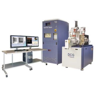
Nanoscale EngineeringFIB Circuit Edit: Specialized front-side and back-side modifications for 5nm architectures and beyond. -
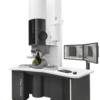
Metrology & CharacterizationAtomic-Resolution STEM: Probe-corrected imaging providing sub-angstrom validation for advanced materials. -
Chemical AnalysisSpectroscopy: High-sensitivity EELS and EDS for precise elemental quantification and chemical mapping. -
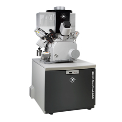
Precision Specimen PrepTEM Lamella: High-yield, site-specific preparation using advanced Dual-Beam FIB systems. -
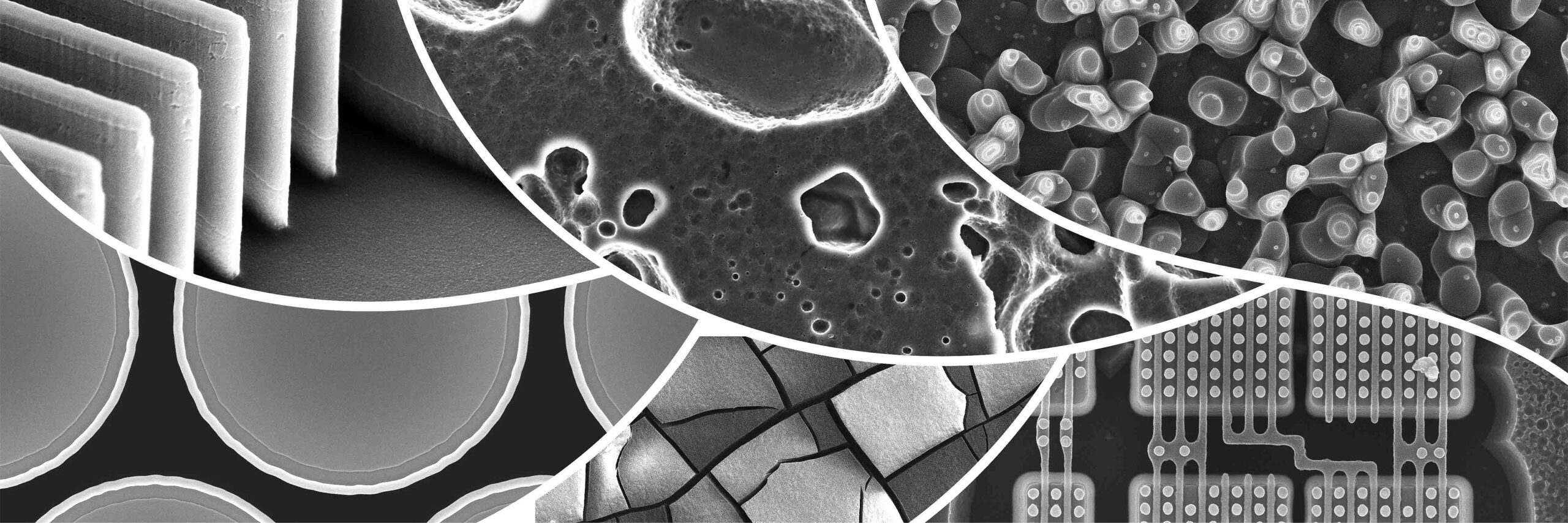
Surface ScienceHigh-Resolution SEM: Quantitative surface analysis for morphology and defect inspection.


