-
 FIB Cross-Section | High-Resolution SEM imaging | TEM Sample Preparation | EDS analysis | FIB nano-machiningDual-Beam FIB-SEM ServicesADVANCED CIRCUIT ENGINEERS, LLC.
Dual-Beam | FIB Cross-section | SEM | EDS
FIB Cross-Section | Dual-Beam FIB-SEM | TEM Lamella Sample Preparation | EDS
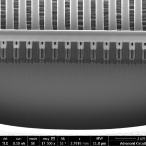
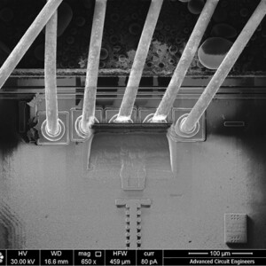
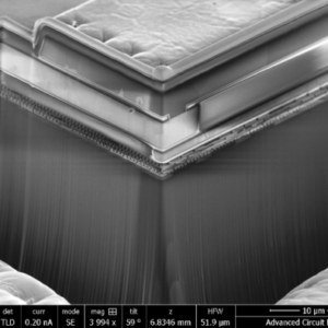
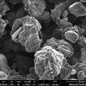
Utilizing the Nanolab 660 Dual-Beam (FIB-SEM), ACE offers a full line of applications ranging from: TEM Lamella Sample Preparation service, Failure analysis Cross-Sections, High resolution SEM imaging, nano-machining, STEM and EDX analysis.
Competitively priced
-
- Discounts for volume work
-
- No “rush-surcharge” expedite fees
- Quick turn-around
Results
-
- High resolution Scanning Electron Imaging (HR-SEM)
-
- 20nm-100nm TEM lamella sample preparation “lift-out”
-
- FIB Cross-Section
- EDX, STEM, ION beam nano-machining
- Electrolytic-Electroless Microvia analysis
Onsite Collaboration
- Feel free to stop by and work with our analyst on your project
Helios Nanolab 660 Dual Beam
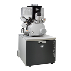
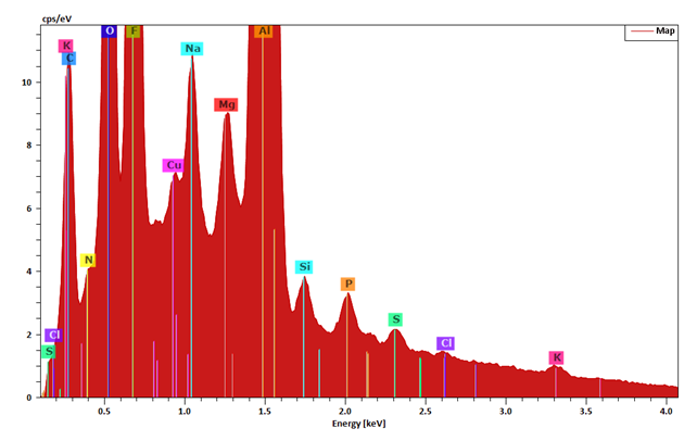
Nanolab 660 System configuration and capabilities
- TEM Lamella Preparation service | ~20nm – 100nm Lamella
- Electrolytic-Electroless Microvia analysis
- Elstar high resolution electron column (1nm resolution) Imaging modes: SE/BSE/STEM
- Sample size – Up to 8” wafer can be loaded through front door; 60% of wafer can be imaged without the need to break or cleave
- Electron and ion deposition of carbon and platinum for site marking and protection during ion milling
- EDS analysis using Bruker Quantax Espirit microanalysis software with XFlash 6/60 detector. Elemental data can be collected in Spectral, Line scan and Mapping modes

