Sub-Angstrom Resolution & Atomic Characterization
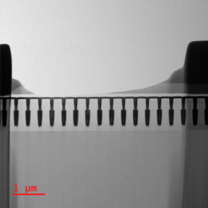
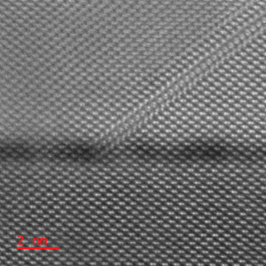
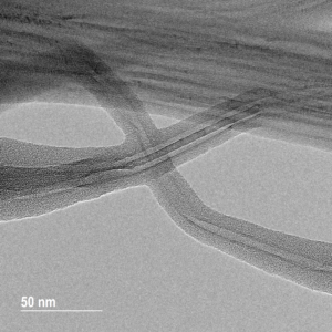
Advanced Circuit Engineers (ACE) provides high-tier analytical services via the FEI TITAN platform. Our laboratory specializes in high-fidelity visualization and quantitative chemical characterization for the most demanding material systems. Our instrumentation provides critical data for multi-layer interfaces, quantum wells, lattice dislocations, and high-resolution compositional mapping.
Hardware Aberration-Correction Technology
The FEI Titan at ACE is a Hardware Probe-Corrected instrument. By physically eliminating spherical aberration at the source through a dedicated S-CORR hardware architecture, the system produces an exceptionally coherent, high-current electron probe. This enables sub-angstrom resolution, far exceeding the analytical limits of conventional TEM systems.
Utilizing high-angle annular dark field (HAADF) imaging, we deliver definitive Z-contrast visualization for material differentiation at the atomic scale. This hardware-level precision significantly enhances Electron Energy Loss Spectroscopy (EELS) sensitivity, allowing for the detection of light elements and subtle chemical shifts that are often lost to resolution blur on non-corrected instruments.
- ▪ Light Element Quantification
- ▪ Chemical Bonding & Valency Analysis
- ▪ Atomic-Scale Elemental Distribution
- ▪ Sub-Å Lattice Imaging
- ▪ Interface & Oxide Stoichiometry
- ▪ Crystallographic Strain Mapping